Industry Overview

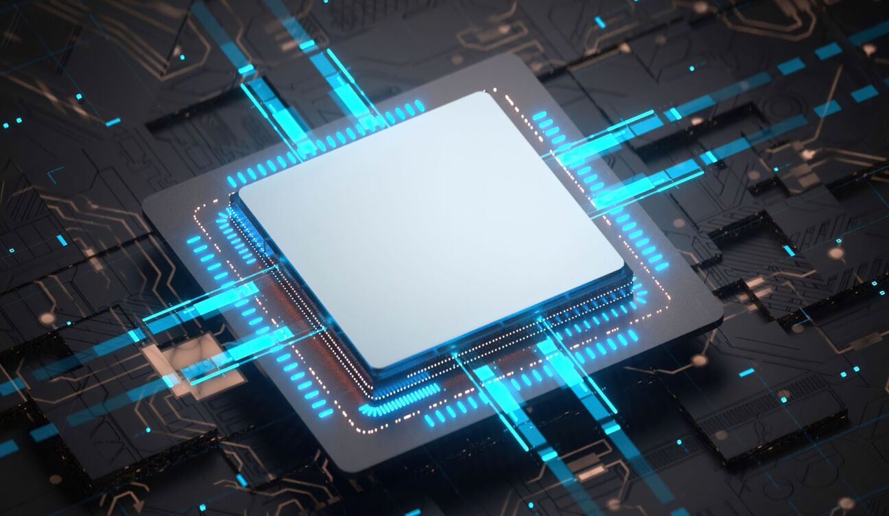
New chip fabrication processes bring exponential complexity to semiconductor design and manufacturing. The entire workflow, from functional logic verification and physical design to optical proximity correction, now relies heavily on HPC and electronic design automation (EDA) tools.
TaiShan HPC Solution delivers a breakthrough by deeply adapting and optimizing leading China-made EDA tools. This significantly improves simulation efficiency, resulting in shorter design cycles and higher manufacturing quality. It is the reliable, advanced technical foundation for your chip R&D and production.
Challenges
Soaring Computational Demands
As chip design advances, the demand for raw computing power to handle EDA simulations grows exponentially.
Fluctuating Workload Demands
Chip design cycles are defined by dramatic peaks and valleys in resource consumption, requiring flexible scaling and efficient scheduling.
Accelerating EDA Innovation
EDA tools require deep integration with computing platforms and hardware-software co-optimization.
Highlights
Superb Performance
Jobs are managed and scheduled across 380,000-core mega clusters, with a throughput of 4 million jobs per hour.
High Scalability
EDA-aware scheduling policies enable dynamic resource scaling to achieve over 90% utilization.
Mature Solution
Several dozens of EDA tools are supported, with hundreds of thousands of cores deployed in real life.
Related Products
Application Scenarios

Chip Design
Chip design transforms system functionality into a concrete manufacturable circuit layout through stages like architecture, logic, and physical design.
EDA tools are vital for chip design. They empower engineers to design, simulate, verify, and optimize circuits efficiently, accurately, and at reduced cost/risk. HPC accelerates the compute-intensive tasks to compress the design cycle. TaiShan currently supports various homegrown EDA tools, including both analog and digital toolchains.

Optical Proximity Correction (OPC)
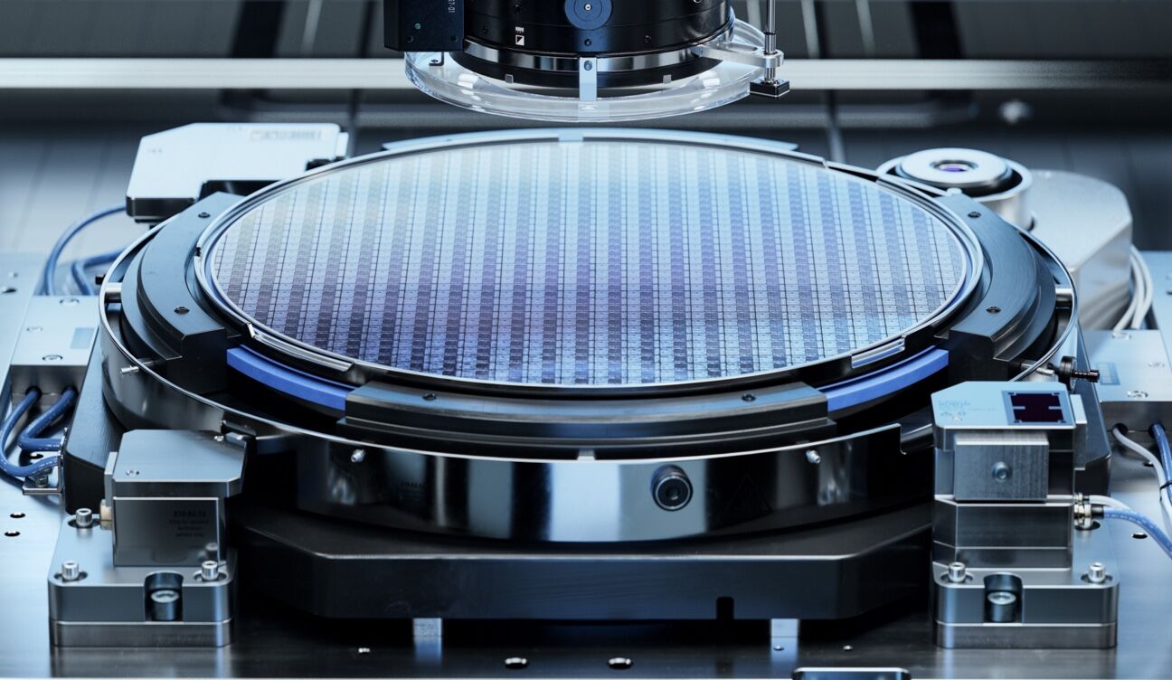
OPC is a critical computational technique used to refine lithography imaging. It drives up resolution and pattern quality to meet the rigorous demands of ultra-fine chip manufacturing.
In this process, EDA software provides essential algorithms and models for simulation, optimization, and validation. HPC is the indispensable engine, rapidly processing massive datasets to accelerate the entire lithography design cycle. This synergy empowers engineers to design with greater efficiency, dramatically boosting both the precision and speed of chip manufacturing.
Application Cases
Circuit Simulator
SPICE is a circuit simulation tool that solves complex circuit equations, leveraging multi-core and multi-threading technology to speed up tasks like direct-current and transient analysis.
Built on SPICE, the circuit simulator combines an intelligent matrix solver with advanced parallel processing to simulate faster without compromising precision.

